| English | 简体中文 |
|
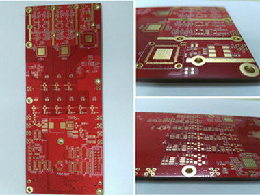
PCB Fabrication
Manufacture capability:
Layers: 1-22 layers
Materials: CEM1, CEM3, FR-4, High Tg FR-4, Aluminum board
Material: RoHS
PCB thickness: 1.6 ±0.1mm
Max. board Thickness: 6.0mm
Minimum hole size: 0.20mm
Minimum line width/space: 3/3mil
Min. S/M Pitch: 0.1mm(4mil)
Plate thickness and aperture ratio : 12:1
Minimum hole copper: 20µm
Hole dia. Tolerance(PTH):±0.075mm(3mil)
Hole dia. Tolerance(NPTH):±0.05mm (2mil)
Hole position deviation:±0.05mm (2mil)
Outline tolerance:±0.05mm (2mil)
Surface finished:Lead free,Immersion ENIG,Chem Tin,Flash Gold,OSP,Gold finger,Peelable,Immersion Silver
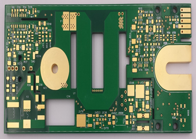
The digital world is getting complex hour by hour whereas the hardware associated with it is getting drastically smaller. The advantages of HDI PCBs are numerous, starting with more interconnections in smaller areas. This results in the miniaturization of boards that can be used in many applications.
The PCB industry plays a prominent role in the development of all the electronic gadgets. PCB made it possible for creating crucial electronic devices.
As the size of the components shrinks, printed circuit board manufacturers adapted to the changing trends. This led to the birth of HDI design. This has made PCBs smaller, denser with higher component count, and faster.
 sales@japcbpcba.com sales@japcbpcba.com  Monday - Sunday : 9:00 - 22:00 Copyright © JA Electronics Co.,Limited Monday - Sunday : 9:00 - 22:00 Copyright © JA Electronics Co.,Limited
|