| English | 简体中文 |
|
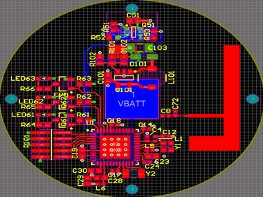
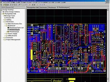
PCB Design and Layout Services
Printed circuit boards form an essential part of any electronics
equipment these days. The PCB design and layout forms an integral part
of the design of the whole product, and it can be the key to the success
of the product meeting its performance requirements in many instances. Maybe
you have a schematic or a frame diagram , but no time or tools to
finishe the design,we can help you to complete your ideas. Our engineers
has the expertise to provide a comprehensive to meet your requirements .
PCBs can be single-sided (one copper layer), double-sided (two copper
layers on both sides of one substrate layer), or multi-layer (outer and
inner layers of copper, alternating with layers of substrate).
Multi-layer PCBs allow for much higher component density, because
circuit traces on the inner layers would otherwise take up surface space
between components. The rise in popularity of multilayer PCBs with
more than two, and especially with more than four, copper planes was
concurrent with the adoption of surface mount technology .
 sales@japcbpcba.com sales@japcbpcba.com  Monday - Sunday : 9:00 - 22:00 Copyright © JA Electronics Co.,Limited Monday - Sunday : 9:00 - 22:00 Copyright © JA Electronics Co.,Limited
|